
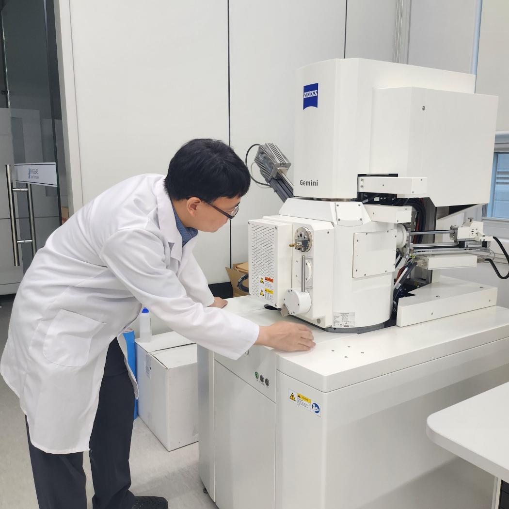
了解亞太地區的材料科學研究人員如何使用GeminiSEM
電子顯微鏡研究創新者系列Learn about ZEISS GeminiSEM's low kV imaging technology
& how it can help your research

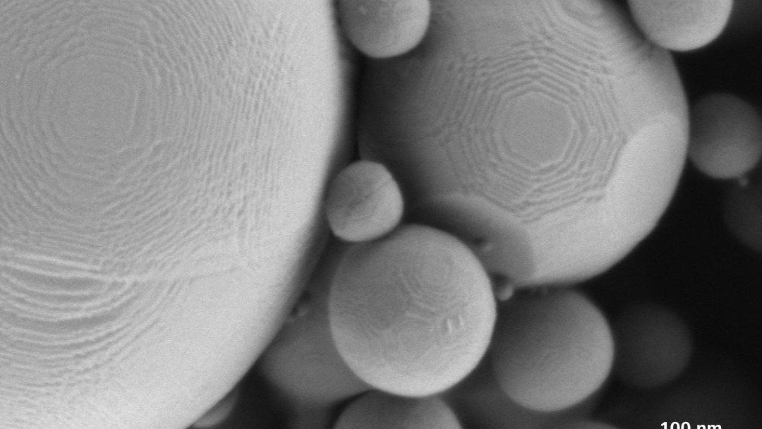
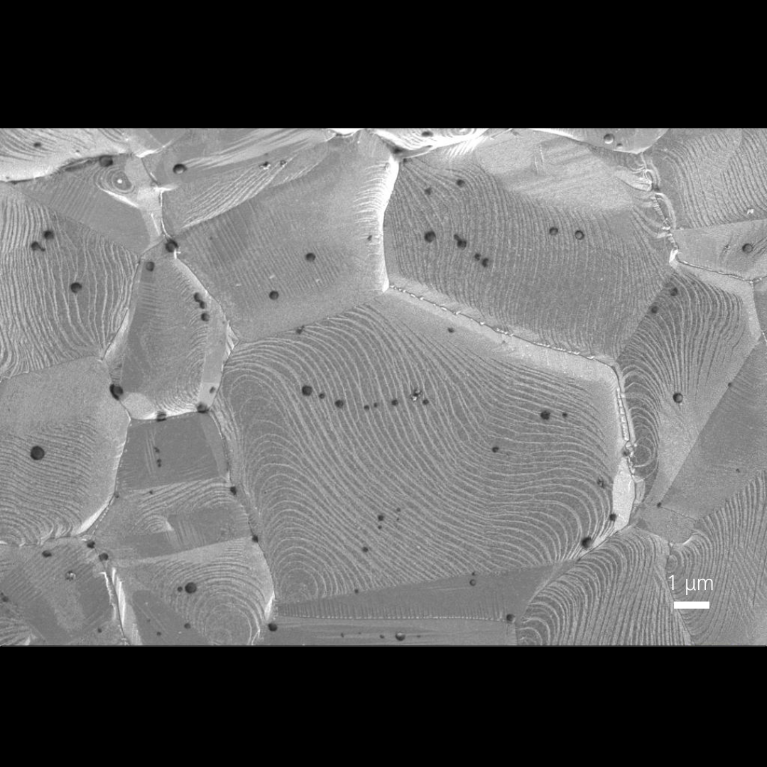
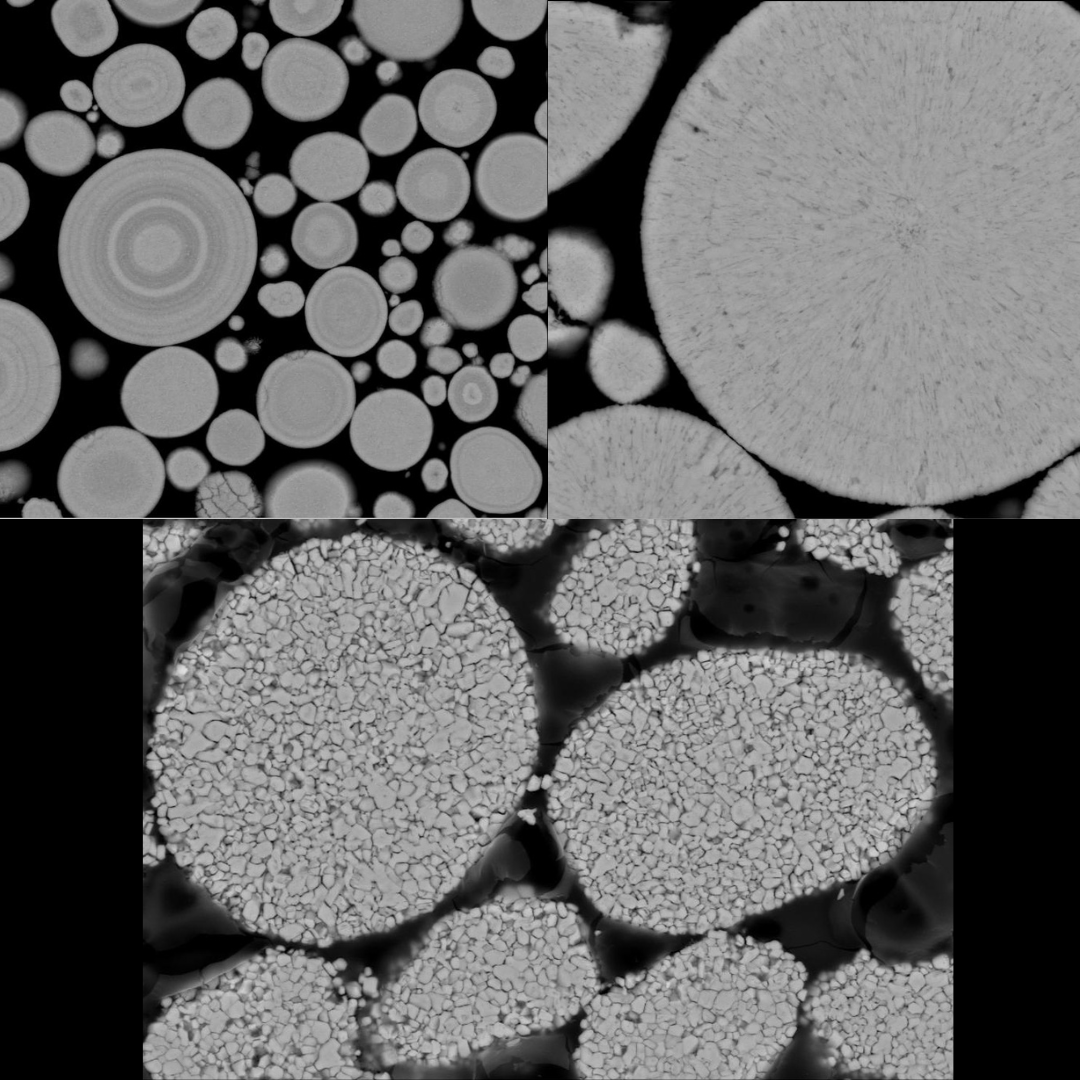
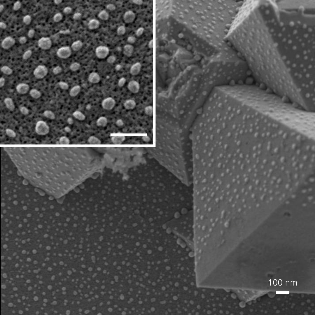
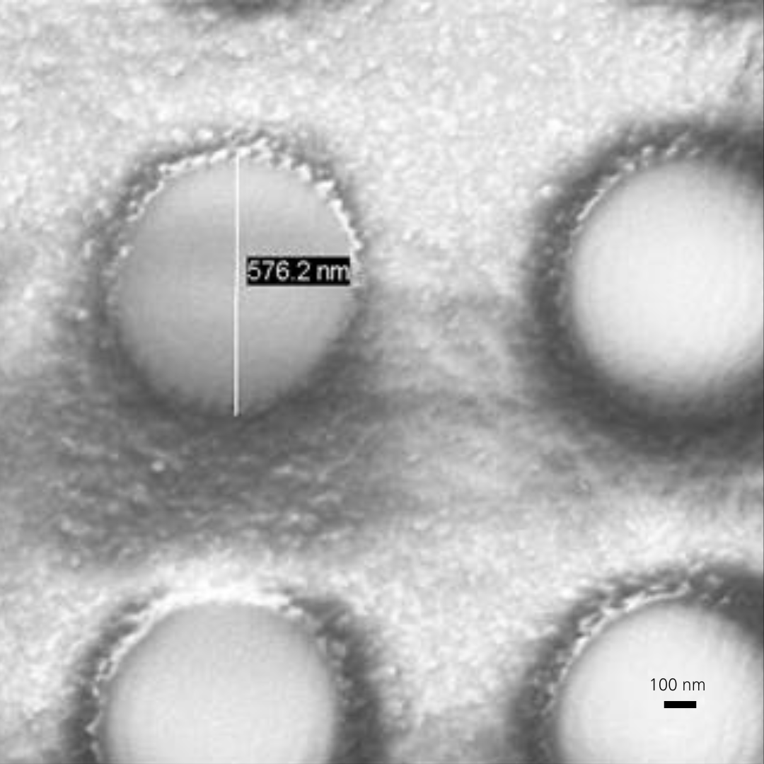
True surface imaging of Alumina 12 at 200V without sample coating or stage biasing.

Achieve true surface imaging of your samples at ultra-low kV
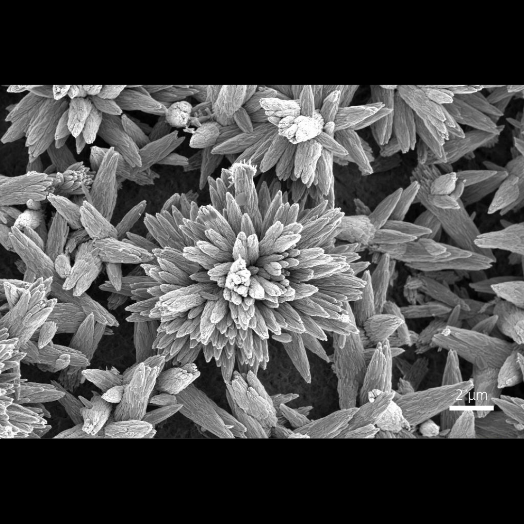
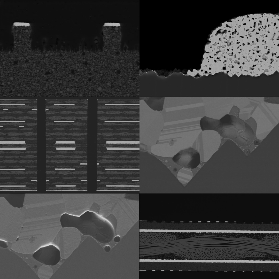
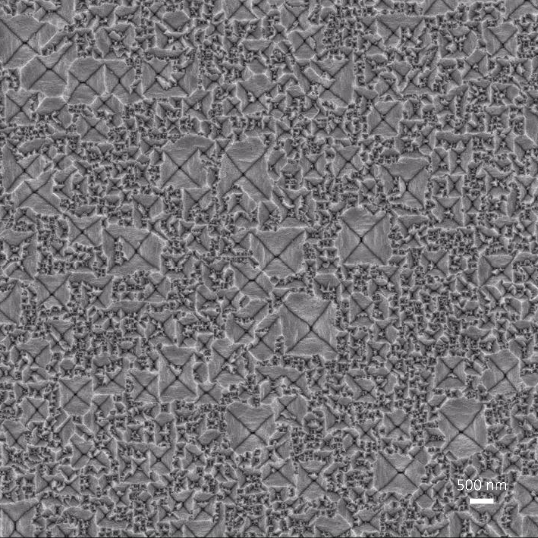
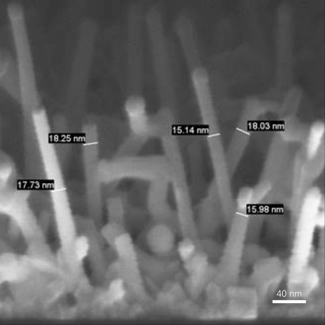
Learn how non-conductive samples such as mesoporous silica, SiC fibers & CNTs can achieve high resolution of highly magnified images. The samples were imaged between 0.5 to 1 kV without surface coating or stage biasing.
See how other researchers are using ZEISS GeminiSEM In the Asia Pacific region
Innovators with different backgrounds from China, Korea, India, Taiwan, Japan & SEA discuss how their users and their organization have benefitted from owning a ZEISS field-emission scanning electron microscope.

Dr. Gong Ming
Deputy director, Lab of mechanical & materials science, University of science & technology, ChinaDr. Gong Ming is using ZEISS GeminiSEM to serve more than 50 major projects of the National Natural Science Foundation, National Outstanding Youth Science Fund projects, National Key research and development programs.

Dr. Keyongsu Jeon
Senior Researcher Daegu Technopark, Technical Infrastructure Support Division Nanotechnology Processing Center, KoreaDr. Keyongsu Jeon is currently researching various types of samples, such as nano-materials/components, ceramics, metals, polymers, bio or semiconductors, from diverse customers (both industries and academics).

Dr. Jae Kim
Senior Researcher Ulsan Technopark, Fine Chemical & Material Technology Support Division, KoreaDr. Jae Kim is currently researching the characterization of materials using scanning electron microscopy. He is particularly focused on the imaging of 3D printing-related polymeric materials, metal powders, and composites.


Dr. Liuwen Chang
Professor, Department of Materials and Optoelectronic Science, National Sun Yat-sen University, TaiwanDr. Chang, who researches electro-epitaxy of metals and compound semiconductors, uses SEM-based techniques such as EBSD, ECP, and ECCI to provide microstructural information of the epilayers in a non-destructive manner.


Dr. Ruma Ghosh
Assistant Professor, E&ECE Department, IIT Dharwad, IndiaDr. Ruma is researching the morphologies, surface compositions, and dimensional analyses of nanomaterials, thin films, metal and ceramic composites, and microbial cells.


Dr. Savitha Purakkat
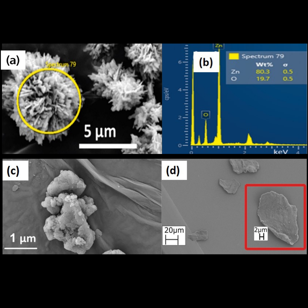
National Nanofabrication Centre, Centre for Nanoscience and Engineering, Indian Institute of Science, IndiaDr. Savitha is currently researching dielectric film like, Al2O3, sub 50nm feature imaging.
Dr. Satyam Suwas
Professor & Chair, Department of Materials Engineering, IISC, BangaloreDr. Satyam Suawas is currently researching deformed and annealed metals and alloys.


Click on the circle markers on the image to open the information box with more details.
Discover the technology behind Gemini Optics


Explaining the Gemini principle in 3 Sentences...
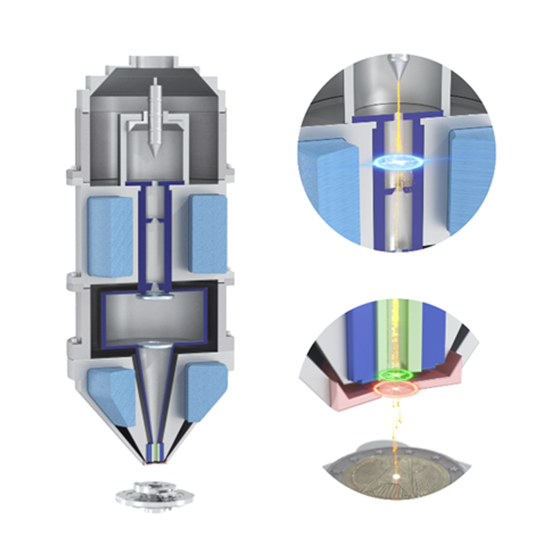
Gemini Optics technology breakthrough
over the yearsZEISS GeminiSEM stands for effortless imaging with sub-nanometer resolution. These FE-SEMs (field emission scanning electron microscope) combine excellence in imaging and analytics. Innovations in electron optics and a new chamber design let you benefit from better image quality, usability and flexibility. Take sub-nanometer images below 1 kV without an immersion lens. Discover how Gemini optics has improved and evolved over time.
-
1993
Gemini 1 |
First FESEM With GEMINI OpticsThe combination of magnetic and electrostatic lens (Gemini optic lens) opens access to the world of low kV imaging. Photoresist and ceramic samples can be imaged uncoated without charging effects at high resolution with the DSM 982 Gemini.

-
2003
First Backscatter Detection (BSD)
at Low kVThe EsB detector is enabling in-column backscatter detection for the first time. The unique energy filtering properties are used to enhance the material contrast. Even nanocomposites can be analyzed with good material contrast with a small interaction volume.
Conventional diode detectors were not able to work below 5 kV, but the in-column EsB can provide this.
-
2004
Introduction of Sweet Spot Imaging
Cazaux and Grillon are publishing results showing the influence of the working distance for selective contrast imaging with the Gemini objective lens.
Sweet spot imaging means systematically varying the SEM accelerating voltage and working distance for optimum image quality.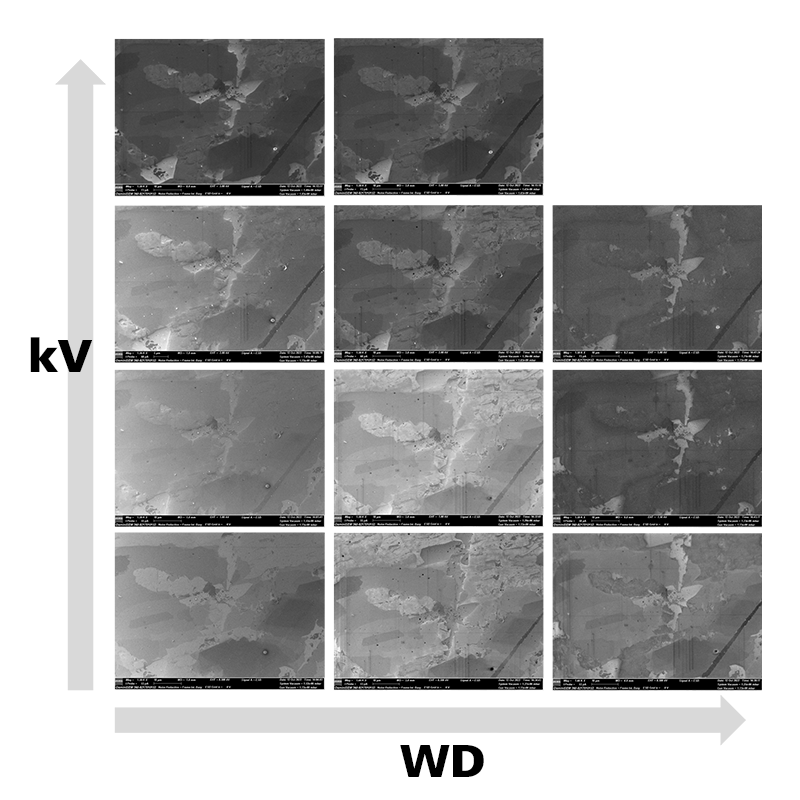
-
2009
Correlative or Multi-Modal Microscopy
Correlative microscopy enables relocating regions of interest (ROI) in specimens in an electron microscope, which were previously identified in a light microscope and vice versa. The entire process takes only a few seconds. This opens up totally new dimensions in microscopy e.g., identification of ROIs with light microscopy and subsequent analytics in the SEM.
-
2010
Gemini 2 |
Double CondenserThe upper condenser sets the beam current, the lower condenser accounts for optimum resolution by optimizing the aperture angle, enablimg high resolution at all beam currents. For a larger depth of field, the system can be switched to a different imaging mode and the convergence angle will be decreased.
-
2015
Gemini 3 |
GeminiSEM with Nano-twin Lens
and NanoVPThe Nanotwin objective introduces a new lens design with lower aberration coefficients. It is optimized for ultra high resolution at low kV.
-
2018
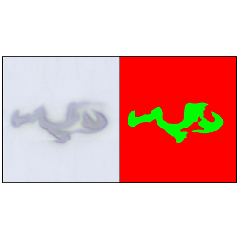
Machine Learning for Microscopy
Zeiss ZEN Intellesis produces powerful machine learning segmentation of multidimensional images. It enables image segmentation and object classification without the need to code a single line.
-
2023
Gemini Optics Is Turning 30 Years 🎉
What an anniversary! Scroll further down to explore which microscopes use the technology, to which extend and last but not least, how the technology that we celebrate today works.
⬇️