

Accelerate your semiconductor packaging failure analysis
Transform your workflows with best-in-class imaging, efficient sample preparation and characterization with ZEISS microscopy solutions
In the More-than-Moore era, the semiconductor industry demands smaller, faster, and more powerful devices, driving the critical role of semiconductor packaging.
The complex packaging architectures, feature scaling and increasing density of interconnects have introduced challenges in reliability, fault isolation and physical analysis.
ZEISS offers new workflows and improves the throughput, success rate and yield with innovative breakthroughs in non-destructive imaging, high throughput sample preparation and best-in-class imaging and analysis capabilities.


ZEISS workflow solutions overview
Here's how we can help
Fault isolation and physical analysis workflows have seen new challenges with the advances in semiconductor packaging technology.
Innovative connected workflows and correlative solutions from ZEISS address some of these new challenges and increase throughput and success rate.
Non-destructive 3D Imaging
ZEISS X-ray microscopy enables non-destructive high-resolution visualization of several defects and failure modes, minimizing physical analysis for known defects. Physical cross-sectioning, imaging and materials analysis is often required for new defects and failure modes. Depending on the failure mode and analysis requirements, conventional sample preparation methods or site-specific rapid sample preparation may be required for root cause analysis.
Site Specific Failure Analysis
Site-specific sample preparation guided by the X-ray data using the laser-integrated FIB-SEM enables fast and precise sample preparation. This workflow is tailored to enhance productivity and turnaround time within minutes compared to hours.
Routine Imaging and Analysis
Sample preparation using conventional mechanical polishing and broad ion beam milling is still relevant for several cases. The optical and X-ray imaging data can be used to direct sample preparation and fed to the ZEN software for fast and easy navigation in ZEISS electron microscopes for routine inspection and analysis
Learn more by interacting with the flashing blue dots below.
Transform your sample prep and site-specific analysis with efficient workflows


Learn more about this workflow below
Advanced package failure analysis using correlated X-ray microscopy and LaserFIB
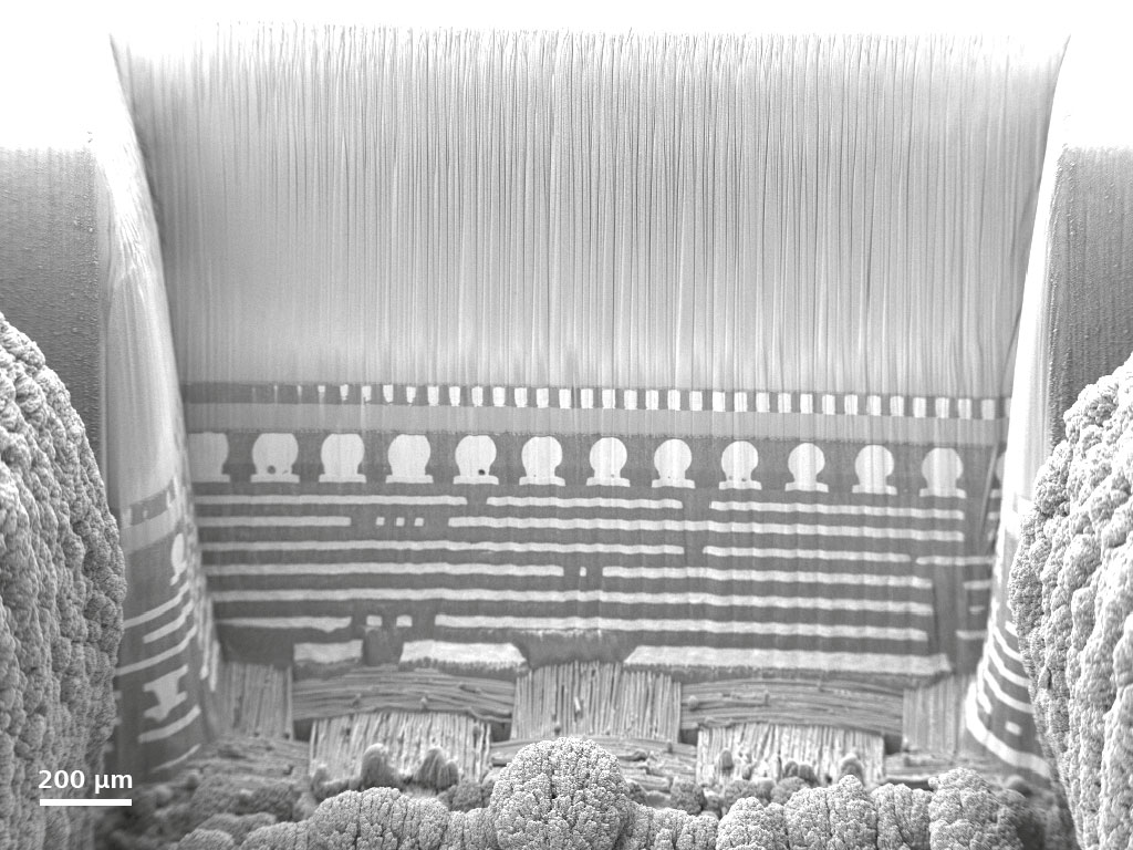
The evolution of packaging architecture with increasing density and scaling of features is resulting in large footprints to accommodate more components and functions that are integral in the heterogeneous integration roadmap and the More-than-Moore era.
These developments pose new challenges in failure analysis and process characterization and drive need for advances in analysis tools, techniques, and development of novel workflows. In this work, we discuss the advances in two classes of techniques that have gained traction in the advanced packaging industry, 3D X-Ray Microscopy (XRM) and laser-integrated focused ion beam scanning electron microscopes (FIB-SEM) for sample preparation.
While the laser integration in the FIB-SEM workflows has improved cross-section preparation throughput, precise targeting for site specific analysis of buried features requires the correlation with a complementary technique to provide sub-surface information.
The use of 3D XRM to guide laser-integrated FIB-SEM analysis presents several advantages to address this challenge. In this work, we describe a novel workflow using 3D XRM and fs-laser integrated in a FIB-SEM (also called a LaserFIB) to precisely target and deliver results at high throughput. This represents a significant development in addressing the challenges of advanced package failure analysis.
Learn more by interacting with the flashing blue dots below.
3D X-ray guided sample preparation for routine inspection


Learn more about this workflow below
Do you identify with any of these problems?


Are you limited by the resolution of your non-destructive techniques to isolate and visualize defects in your large package?


Are you challenged by the poor contrast of your X-ray CT to see underfill voids, delamination and cracks?


Is your current sample preparation process taking days or introducing artefacts?
Pick a solution that interests you
-
Non-Destructive 3D Imaging
Using ZEISS XRM


ZEISS Xradia Versa 3D X-ray microscopes (XRM) provide non-destructive imaging at submicron resolution. 3D visualization with unlimited 2D "virtual cross sections" from any angle allows deep insights to identify defects and failures on intact samples while preserving sample integrity.
Dual-stage magnification and RaaD™ technology offer high resolution even for large packages breaking the sample size limitations. The intuitive software allows easy navigation and acquisition at any site in the sample.
AI-enabled reconstruction ensures high-speed data acquisition and high contrast imaging breaking traditional barriers of field of view, resolution and throughput.
The unique architecture and AI-powered software allow you to minimize your cost per sample while providing the best in class performance.
-
Imaging & Analysis
Using ZEISS FE-SEM

The ZEISS Sigma and Gemini SEM family are state-of-the-art field-emission scanning electron microscopes (FE-SEM) combining subnanometer resolution and excellent contrast of materials.
The large chamber with sufficient ports allows the addition of several analytical detectors for material composition and grain analysis.
Its versatile capabilities are well suited for a wide range of applications, including construction analysis, failure analysis, passive voltage contrast, subsurface analysis, electrical measurements with probing and material characterization.
The microscope's ease of use and software portfolio allows seamless integration in multi-tool environments, improving workflow efficiencies.
-
Sample Preparation
Using ZEISS Crossbeam Laser
The ZEISS Crossbeam FIB-SEM is a highly efficient sample preparation tool combining Gemini imaging with the high-performance Ion sculptor Ga-FIB.
Integrating a femtosecond laser offers rapid generation of high-quality cross sections of large interconnects and BEOL structures buried down millimeter deep in a 3D integrated circuit (IC) package.
Combining with 3D X-Ray data, precise targeting of sub-surface features is routinely achieved. The crossbeam offers superior high throughput 3D serial section imaging and TEM sample preparation workflows.


